Printed electronics have introduced huge advantages to the production of electronics, especially related to the deposition and utilization of functional materials. While problems with deposition remain, for example, the clogging of printer nozzles and the relatively complicated process of producing the widespread nanoparticle-based inks, inkjet printing as an additive method has clear advantages such as efficient use of materials, low energy consumption, and the absence of large amounts of harsh substances.
What has remained largely untouched by the printing revolution, however, are approaches to the curing of metal layers. The conventional way is to use heat, which can damage delicate substrates such as paper, textiles, or polymers. As a result, while metals can in principle be printed onto nearly every material, established curing methods limit the range of substrates that are effectively used for printed electronics.
First answers to this curing challenge start to emerge. Newer approaches for room-temperature processing use UV light and high-energy photonic light. For silver inks, there is also a chemical process of forming a metal layer based on Tollens’ reagent. Still lesser known is a novel technology using cold plasma which turns precious metal inks into high-performance metal layers. Even better, the inks that this technology requires are nanoparticle-free. So the technology hits two birds with one stone - improved processing and avoiding nanoparticles.
Printed electronics and the curing challenge
The advantages of printing electronic components are too numerous to list them all. Where frequent changing of pattern is a must, such as piloting, the advantages are obvious. But even for mass production, a concise and material-saving process (metal application is additive, not reductive) has advantages that are hard to ignore, especially when printing with expensive precious metals such as platinum or gold. Finally, with the environmental footprint of production processes getting more and more attention, low-waste printing techniques increasingly gain importance compared to “traditional” metallization techniques.
Unfortunately, the gains of printing come at a price. A commonly known is the price of materials. Even the most sophisticated metal inks are still based on nanoparticles. The production of nanoparticles is time and resource-consuming, and the process produces significant chemical waste. While for the most widely used silver nanoparticle inks production cost may remain within reasonable limits, prices of inks with palladium, platinum, or gold nanoparticles can be prohibitive.
Cost aside, printed electronics face a number of process-related challenges because of which printing is unlikely to ever outperform large-scale sputtering lines, e.g. for ITO applications in display production. While some first movers in the display industry are experimenting with printing lines, this is still a niche phenomenon. Reasons include that printing is still much slower, especially when the market-dominating nanoparticle-based inks clog printheads every so many meters forcing the production line to be stopped. The other “showstopper” for continuous R2R occurs wherever the printed inks require heat-based curing. Drying times are several minutes up to one hour long, which interrupts even the slowest R2R flow.
So notwithstanding many obvious advantages, common techniques for the printing of electronics still face challenges related to inks and processing, and there is a curing challenge that deserves closer attention.
Alternatives to heat-based curing
One promising alternative to curing with heat is light-based processing like UV-based curing and photonic sintering. Available UV inks are high in viscosity and therefore suitable for high-speed techniques such as screen printing, flexography, and rotogravure. UV light curing can happen at low temperatures and relatively fast. It is successfully used e.g. for printed RFID antennas. One challenge to overcome with UV inks is enhancing the purity of the resulting layer. Light-cured coatings contain a significant share of polymer residuals which impairs functional properties, most notably conductivity per volume.
Photonic sintering is unbeaten in terms of speed. The ink reduces to metal within microseconds. However, the stress on the substrate is locally similar to heat-based methods due to the high-energy nature of the light source. This makes the second main drawback apparent: the high cost and negative environmental impact of high energy consumption.
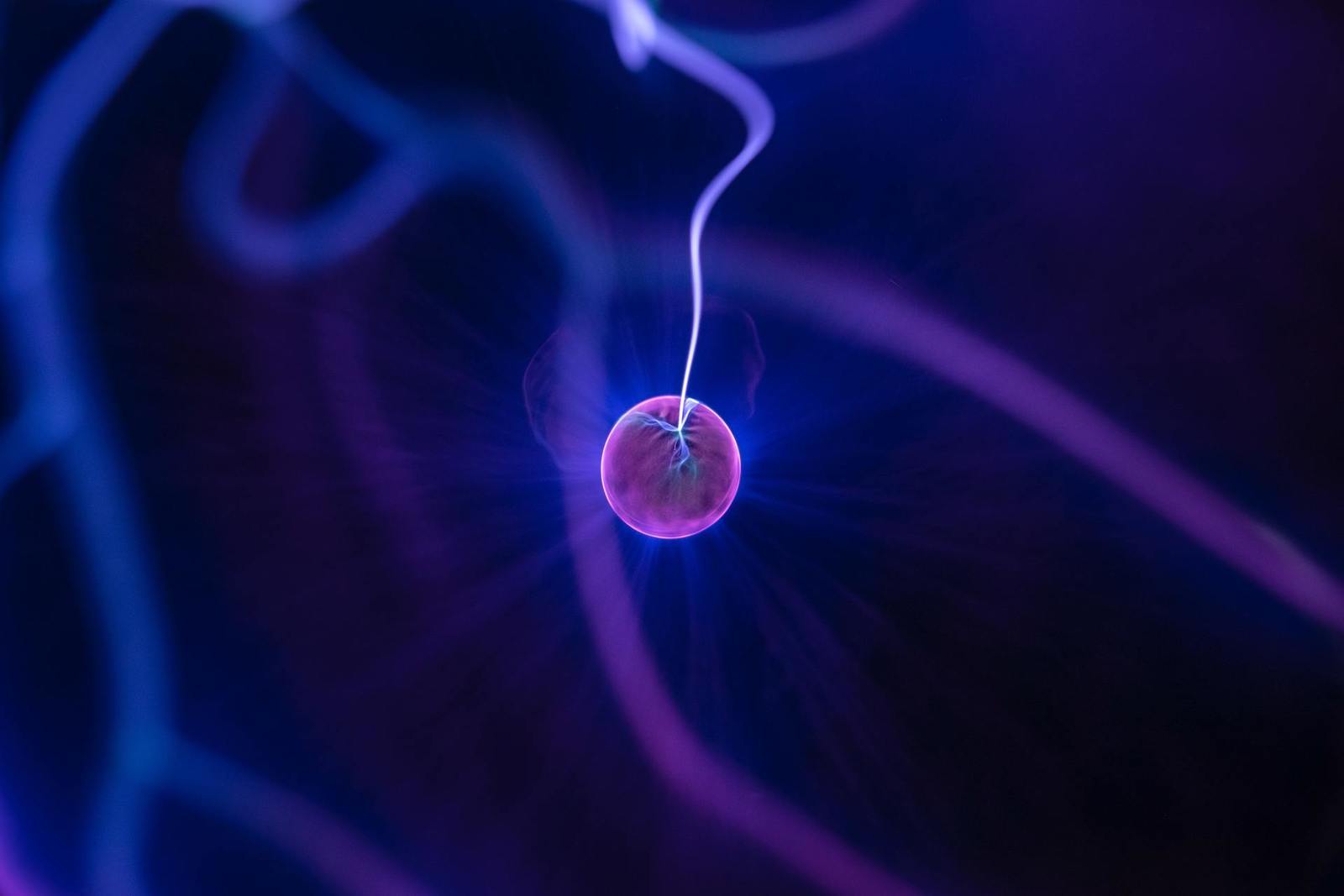
A relatively new alternative to heat-based curing is the use of cold argon plasma. This technology may sound deceivingly complex, but in fact, it is not. Plasma is already widely utilized in the industry, most commonly for cleaning, surface activation, or in some other production step and the machines needed for the plasma curing are the same already widely implemented machines, so-called “plasma cleaners” or “plasma etchers”.
Plasma can be a very gentle surface technique, often affecting just a top few atomic layers, changing their chemical nature or completely removing them. The gas temperature of cold plasma barely exceeds ambient conditions, and the treatment is used not to burn the surface, but to modify or activate it. That is why it is perfect for the activation of sensitive, functional materials.
When used as a conductive ink processing technique, metal layers are achieved at temperatures below 70°C under fast processing times and without chemical waste left behind. An additional advantage is the overall degree of control over the treatment process. Plasma systems are turned on and off instantaneously, and the parameters are easily tunable. Finally, the process enables an even coating of non-flat, porous, or 3D structures, offering to replace certain processing steps of another industry that has well-established methods and processes, of course, none of them flawless - namely electroplating.
Given the cuts on energy use, processing times, and overall low-waste, plasma curing is by far the greenest known curing technology.
Next-generation metallization? – Rethinking ink formulation and curing
A highly interesting metallization technology combines the advantages of plasma-based curing and nanoparticle-free inks. It has been developed by scientists formerly at the Weizmann Institute in Israel and has, as the proprietary core technology of Berlin-based company OrelTech, started to prove to be a solution of choice for applications ranging from simple printed electrodes, printed devices like (flexible) OLEDs and solar cells, gold electrodes for biosensors and e-textiles. It is even used in plating on plastics for direct metallization of plastic parts to create protective, catalytic, and decorative coatings. The ink portfolio currently available contains silver, palladium, platinum, and gold.
So what is the essence of this technology? As previously stated, the two obvious differentiating features are the absence of nanoparticles in the ink formulation and plasma curing. During the process, a near-100% pure metal layer is directly grown on the substrate. This is fundamentally different from nanoparticle layers. Think about the difference between snow and ice. A layer formed of nanoparticle inks resembles snow: many singular particles sit more or less loosely connected on top of the substrate. In layers formed with OrelTech inks, metal is like ice - it grows directly on the surface and forms a uniform layer. This often leads to better adhesion, better cohesion, higher stability, and lower surface roughness. In practical terms, this means the metal layers are thinner, more flexible, and can even be transparent while maintaining high levels of conductivity.
As for the curing, the only process step required after applying the ink is exposure to an argon plasma with slight underpressure (no strong vacuum needed) for times as short as 2 minutes. Therefore, the technology can be run on continuous R2R lines at moderate speeds. Sheet-by-sheet and stack-by-stack (S2S) processes are even easier to implement.
Whether OrelTech’s nanoparticle-free inks are the technology for next-generation metallization remains to be seen. They certainly offer an innovative alternative to existing technologies, especially where heat is a problem for the substrate, functional properties such as conductivity, purity, flexibility, and transparency are important, and where precision in production is more important than speed.
This article was originally published in Specialist Printing Worldwide magazine, Issue 1, 2022.