Although the term “printed electronics” goes back to the 1970s, the modern variant of this field is unimaginable without a technological milestone called “conductive inks”. The pioneers of this innovation, such as S. Magdassi and J. A. Lewis, made breakthrough after breakthrough with metal nanoparticle inks (NP inks), a complex mixture of tiny metallic particles dispersed in organic stabilizers, surfactants, levelling agents, adhesion promoters and more. The result is often a viscous paste, that can be deposited onto a required substrate and then heated to a high (but still not “metal-melting” high) temperature to solidify. The resulting metal-containing layer conducts electricity and thus can be used in printing electronics.
After this knowledge has been fully transferred to the industry and became a staple of printed electronics, the generous waterfall of technological breakthroughs has slowly come  to a halt. There were notable variations to the theme – utilization of smaller particles, smarter and even more convoluted organic mixtures aimed to reduce the curing temperature and improve their usability, different attempts to heat the pastes faster and in a more efficient and controllable way than “your grandmother’s old-time oven”. Some of those did improve the overall process, but none of those changed it. This metal deposition system, while being trailblazing in its time, nowadays leads to a situation that I call “The Vicious Triangle of Printed Electronics”.
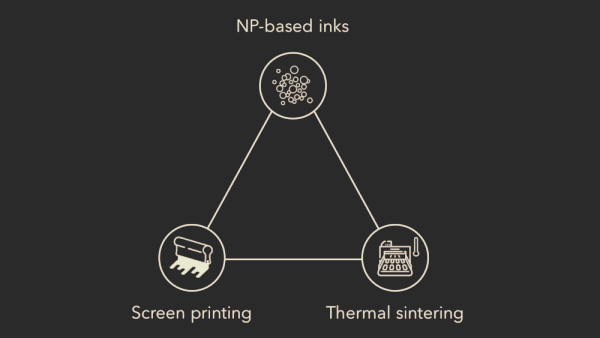
The Vicious Triangle, naturally, consists of three vertices. The NP-based conductive inks comfortably occupy the top vertex. The most common variant that you would see in actual device production is a thick brown paste, which due to its viscosity can only be deposited by our second vertex – a screen printer. A third vertex is what sinters the paste, and it is still, most commonly, a simple oven, or, in more general terms, a thermal sintering process. This is how the absolute majority of printed electronics manufacturing looks like.
The Vicious Triangle of printed electronics
But what makes this triangle, well, “vicious”? A combination of two factors. The first reason is: in most cases, you cannot replace just one vertex – you have to change all three at the same time, and that sounds just too risky for many manufacturers. And the second reason is: for each of the vertices, there already is a better solution on the market, but the manufacturers miss out on them because of the first reason. I will quote a recent IDTechEX webinar “Conductive Inks: Innovations for New Applications” that took place on Jan 12th, 2023:
How can ink design help customers reduce costs?
- Increase conductivity – reduced the amount of ink required
- Maximize printing yield – make ink long-lasting, tolerant of processing variation
- Ink formulation – use solvents that are easy to dispose of, reduce processing temperatures
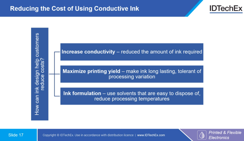
Screenshot from a recent IDTechEX webinar “Conductive Inks: Innovations for New Applications” streamed on Jan 12th, 2023
It is very easy to see, that all three points are directly blocked by one or more vertices of “The Vicious Triangle”. For instance, increased conductivity could be achieved by adding less NP-stabilizing additives, but this would not work because they are needed to make the NP inks screen printable. Better printing yield could be achieved by implementing inkjet or aerosol printing instead, but that is not feasible with current NP-based inks. And switching to more disposable solvents would be possible, but the NP inks require certain stability to be screen printed, and only high-viscosity, high-boiling point solvents can achieve that. You cannot change only one part of the triangle. It sits, monolithically, in the bottleneck of the proverbial technological bottle.
You have to get rid of the triangle completely.
If you stop committing to “The Vicious Triangle”, it’s suddenly feasible to achieve all three points from the IDTechEx webinar, and many more. The inks should be nanoparticle-free. That would immediately allow you to use more “disposable” solvents and make the inks much more stable. Inkjet or aerosol jet printing is a much better alternative to screen printing, since it gives not only high speed, but also huge versatility and processing variation, and they work much better with NP-free inks, due to significantly lower nozzle clogging. And the sintering, or in this case, curing, should be done not by temperature, but by chemistry or electricity. Or, even better, by their combination, plasma.
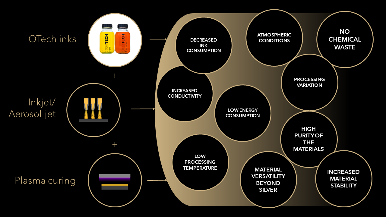
OrelTech technology allows breaking out of the constraints of legacy processes
For the last five years, COVID and all, OrelTech has been developing an alternative system. It is significantly more energy efficient, both during ink production and ink curing, it is utilizing existing printing and plasma technologies, and is optimized for existing and scalable inkjet/aerosol printers and cold plasma etchers. But, even more importantly, it brings a unique versatility, so missed in NP-based inks. Developing a new ink, or even a new printable metal has never been faster, and we are happy to demonstrate it with our family of precious metal inks: Ag, Au, Pt and now even Pd inks are available for direct purchase. Our winning strategy is not just material retail – it is leading the customer all the way from the first feasibility test to a fully set production line.
The ”Vicious Triangle” has been circumvented. The bottle is open.